Motivations
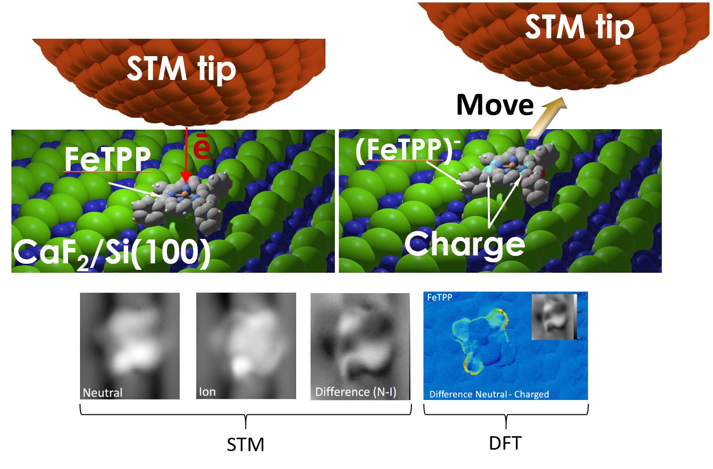
My research is mainly focusing on the study of molecules and atoms adsorbed on semiconductor surfaces to build small molecular architectures for the development of model devices.
This research is aiming at understanding the fundamental aspects of the device properties dealing with their electronic, chemical, magnetic, optical or purely quantum aspects. Ultimately, we wish to exploit these molecular assemblies to create functions and study physical processes in relations with specific or new nanoscale laws.
With scanning tunnelling microscope (STM) working in ultra high vacuum at low temperature (9K), we can control the conformation, the environment and, thus, the general properties of these devices.
Higlight - New Publication !!